Single-Chip Upgrade to Existing Electronic Assembly - aka: Making Frankenstein

The Ask #
For a recent project, my engineer asked me to assemble a prototype that contained a development board, a test fixture, and a customer’s current board design. Our software developer wanted to demonstrate that in order to deliver the desired software capabilities with the customer’s current design, a more advanced module with increased FLASH/RAM and improved range was necessary. The initial module, Fanstel’s BM833A 24KB RAM were not cut out for the design specifications. Luckily, Fanstel had another module, the BM833, which had the same dimensions and footprint with 128KB RAM that could do the job. We just needed a way to show that to our customer.
In an ideal world, we would have a proper board-assembly house put together a production run with this new BM833 module. But of course that is time and cost prohibitive, especially in a situation where the customer was not convinced that upgrading the Bluetooth module was worthwhile. Plus, there were some other minor additions our engineer wanted to make for the next proper revision of this board. So I needed to find a way to do this with the materials I had at hand.
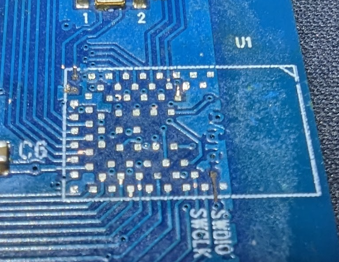
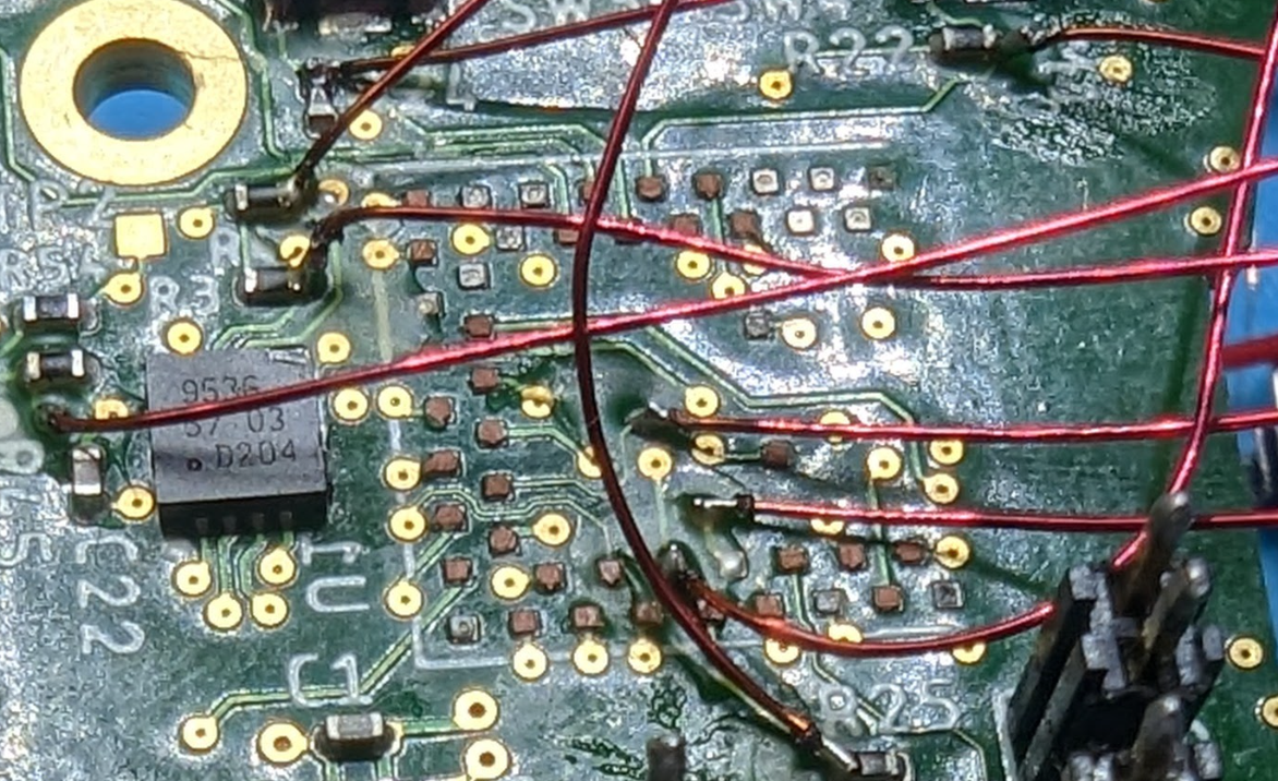
DigiKey describes the package/case for these particular modules as a “68-SMD.” Essentially we are dealing with the same issues with this module that we see with BGA components; lots of tiny, fine-pitch pads smaller than the tip of a pen. They must be precisely aligned in order to make the proper connections. And, they are all beneath the module in places untouchable by my soldering iron.
Even without a stencil for this uncommon footprint, I may have been able to put down some solder paste, place the component, and reflow successfully. But, without an X-ray to verify if the connections were made, and a very limited number of these pricey modules, I decided to take a different approach.
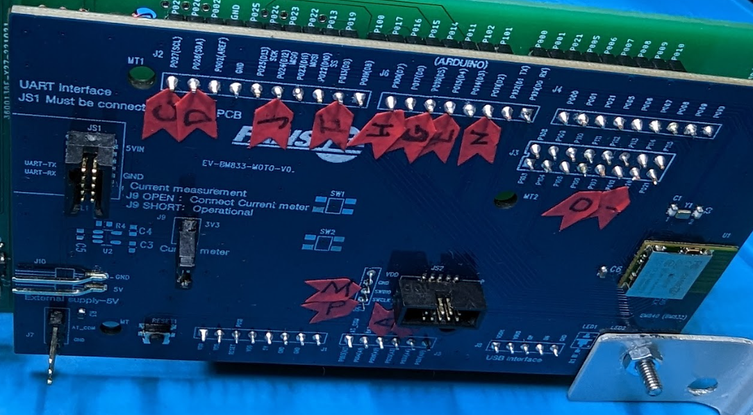
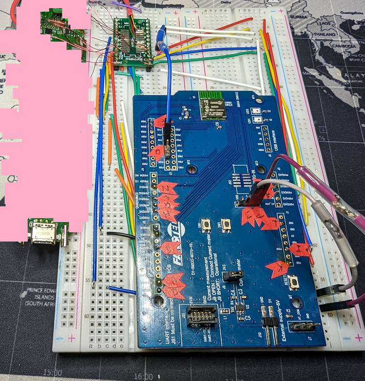
With a pin-out table from my engineer, and the goal of getting something our software developer could test ASAP, I rummaged around my tools and decided to use a good old-fashioned breadboard, and an arbitrary surfboard with enough pads to suit my purposes, and a development board (EV-BM833) that contained the module I needed. Sometimes, I feel like a goofy third grader when I use breadboards amongst my electrical-engineer colleagues, proudly showing off my macaroni art while they are doing PWM analyses. But in this situation, the breadboard was the best way for me to get a quick assembly together while also preventing mistakes. And even if I did make a mistake, it would be just a matter of moving some jumper wires rather than delicately cutting traces and cautiously soldering wires onto a small, crowded board.
I started by meticulously indicating the pins my engineer specified with stickers, so I could have a visual of where I would need to align the development board on my breadboard. Luckily, the pitch of most of the header pins on the development board lined up with the breadboard pitch, so I could plug it in directly, needing to only gently bend a few pins in order for it to sit snugly.
Although I perhaps could have saved some time by just using quick flexible jumper wires, I opted to take the time to create pre-cut wires at the lengths I needed and to keep my signal colors distinct and consistent, like a perfectly-measured and color-coded rainbow. And, if I had to ship this to the customer later, this configuration could withstand that journey. Although, as I had to navigate other issues I did have to add a few flexible jumpers.
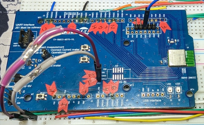
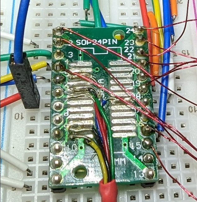
Now I wanted a way to connect my breadboarded signals to the customer’s board. Because of the nature of the BM833 footprint, I concluded that I was just going to have to carefully solder some small-gauge coated wire to the necessary pads. But then where to route the other end of the wire? I found a SOP-24 breakout board with a nice comfy pitch of 1.27 that I could use. With header pins added, it plugged neatly into my breadboard, and I now could solder my coated wire onto the pad or header pin as it suited me.
I still had the delicate task of soldering wires to the pads I needed from the BM833A footprint on my customer’s board. As it turned out, there were some points where it made more sense to attach to a passive component for the signal than the actual pad; a luxury usually only possible when you can review all of the engineering design files.
Those were the primary steps I took to get this initial prototype to our software developer. But as always, upon testing, we ran into a few issues we had to troubleshoot away.
Based on software configurations for the development board, a few of the pins had to be switched around from the pin-out; easy enough to do with the breadboard configuration I had.
Then, our engineer suspected that some of the extra components on the dev board were changing the module’s behavior, so those were removed, basically just leaving us with the module and a few connectors.
Finally, there was an initial J-Link breakout board our engineer designed for this project to go to a header for a serial debug terminal, and that needed to be integrated into this prototype.
Although the team playfully chided me, and nicknamed this prototype “Frank” (as in Frankenstein’s monster), I am mostly satisfied with my use of a breadboard here to deliver a quick prototype that was a key “proof of concept” for the software development side of this project. Although my engineers think Frank is ugly, I think he’s pretty cute. Putting Frank together gave me the time to later assemble a much slicker and sturdier prototype. But the story of that prototype will be for another time.