What Not to Do When Laying Out a Boost Converter

Introduction #
Recently, I was tasked with designing a board that would include several boost converters to drive LED strings. After testing the prototype boards, I noticed numerous stability issues with the boost converters. Investigating these problems led me to conclude that my PCB layout was the main culprit. I want to address these layout issues with you using a real prototype design for an actual product.
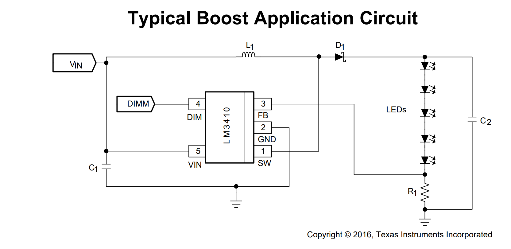
Let’s introduce the chip I’m using and describe its pins. The LM3410 is a constant current boost converter designed for driving LEDs and in this design I will be using it in its typical application. Here are its pins:
- Pin 1: SW: Output switch. This pin switches to ground to drive current through the inductor and the inductor drives current through D1 when the switch stops
- Pin 2: GND
- Pin 3: FB: Feedback pin. The IC acts to keep this pin at 0.2V. Therefore, a constant current is achieved through R1
- Pin 4: DIM: This is an enable and can be used to control brightness via a PWM signal
- Pin 5: VIN: The input power for the chip
How it all Went Wrong #
Now let’s take a look at how I laid it out on the PCB:
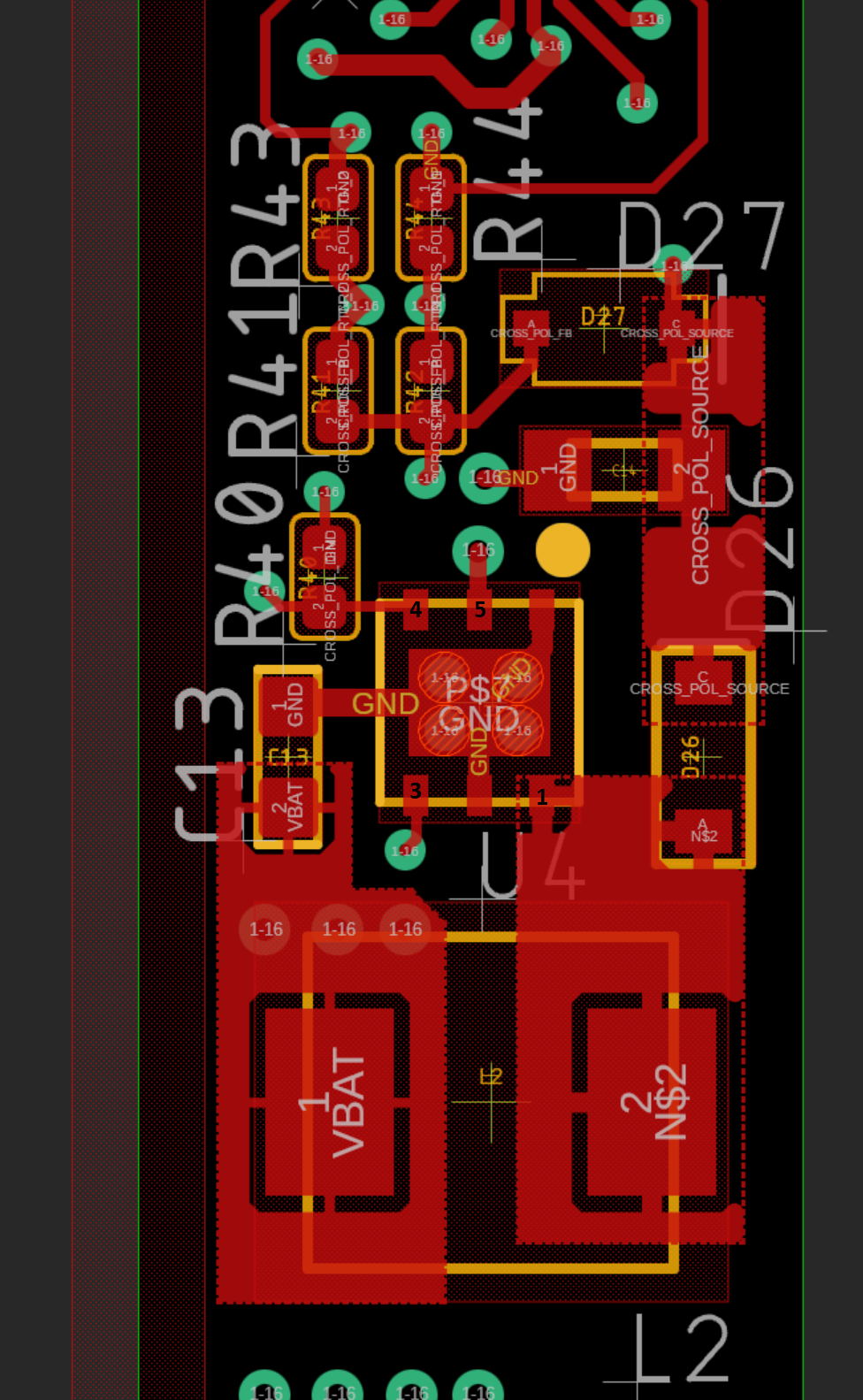
While troubleshooting the stability issues, I returned to my layout. It soon became evident that there were several areas that needed some improvement.
- The first issue I found was that Pin 5 was not being decoupled properly. Observe that the positive side of C11 was not in proximity of the pin it needed to decouple. Pin 5 is the power supply for the chip including the internal switching transistor for the boost converter. The electrical journey from the via that feeds pin 5 to the vias for the VBAT node of C13 is excessively long. Long loops like that add inductance, diminishing the capacitor’s effectiveness.
- The datasheet recommends a common ground plane to connect C4, C13, the sense resistors, and the chip itself. This is done to prevent ground bounce which causes inaccuracy and instability. If the ground of the sense resistors is at a higher voltage than the ground of the chip, then that will cause the voltage at the feedback pin to be inaccurate. Note that in my design, many of the grounds take a circuitous journey through vias before getting back to the center ground pour of the chip.
- Having a larger ground plane also serves a dual purpose; heat dissipation. This chip gives off a lot of heat and a larger ground plane will improve dissipation and promote better thermal performance.
Things got Better #
Let’s look at how I improved the layout below:
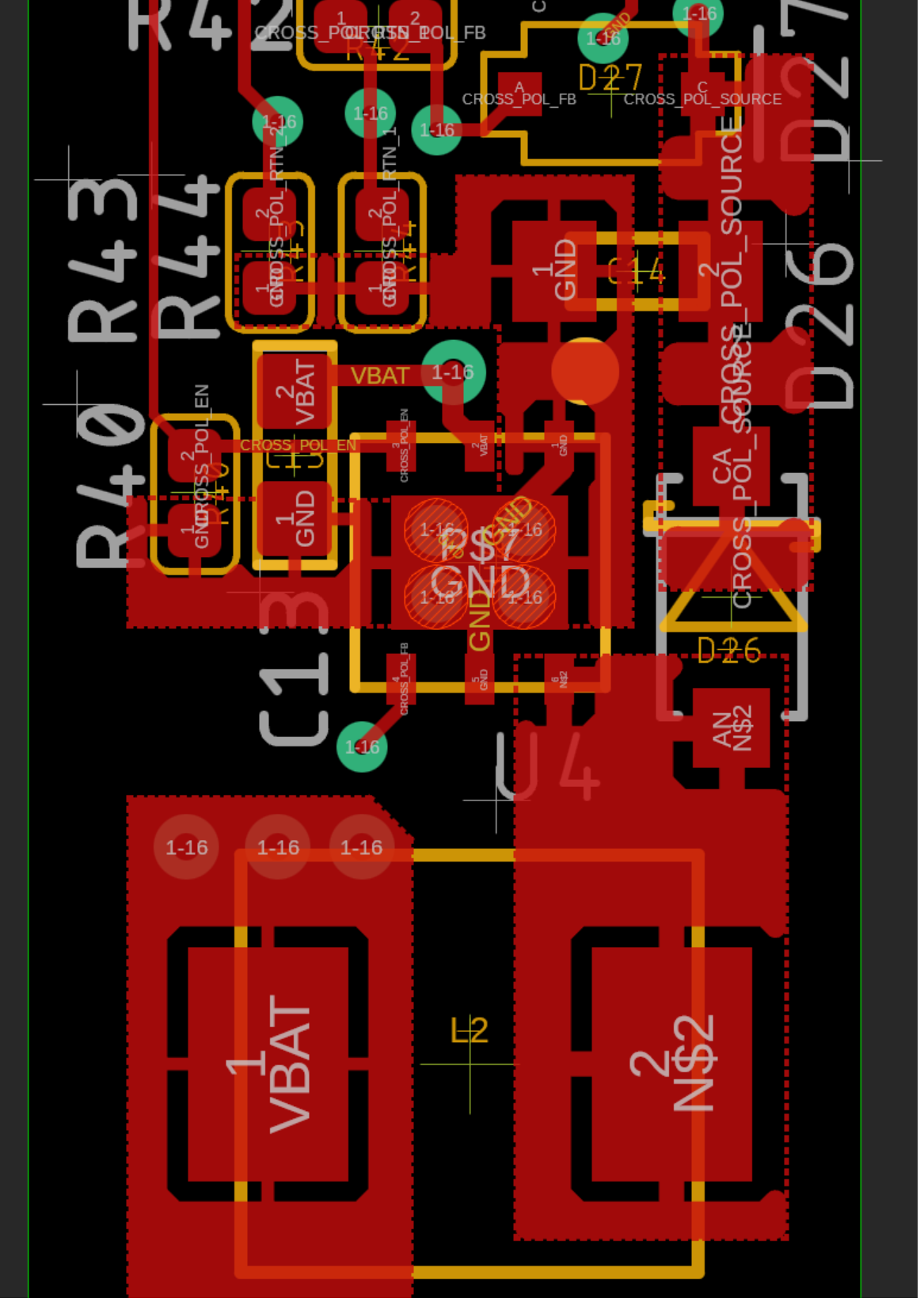
This improved layout includes a common ground plane for all the components and a more direct path for C13 to decouple pin 5. The thermal performance is also improved with a larger ground plane.
To conclude, let’s consider the importance of following thoughtful layout practices for optimal performance. I advise designers to always take a look at recommended or example layouts for their chips. And with inspiration from studying well-executed layouts, we can improve the stability, efficiency, and performance of our designs. I will be paying careful attention to those in the future.